Digilent Atlys Resources
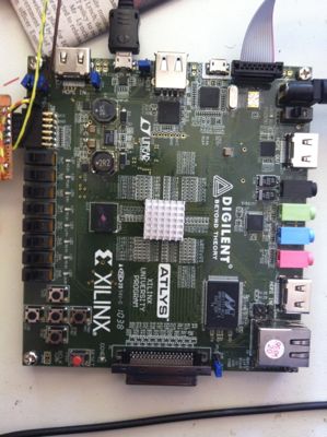
The Digilent Atlys is a pretty good board! It has a nice, high speed VHDCI connector, gigabit Ethernet, HDMI, and DDR2 memory. Unfortunately it suffers from a manual with some glaring errors (including a misspelling of 'FPGA'), an Ethernet chip with an impossible-to-obtain datasheet, and a reference design that was created using the SDK. For those of us using ISE, read on!
Ethernet
I wanted to use the Gigabit Ethernet interface to send data (ideally in UDP packets) to a host computer at high speed. Most HDL experts say that this should be possible without using a microcontroller. They're right, but it's a big pain for several reasons.
Xilinx supplies a triple-speed Ethernet MAC core, TEMAC, but it requires a license, and if you had the money for one of those you could be using a Microblaze soft core and thus Digilent's reference implementation. Opencores.org has a gigabit MAC but I couldn't make much sense of it, which I find is pretty typical of my experience with the site.
Turning to a physically realised design that uses Gigabit, I delved into the USRP2 software defined radio's HDL and firmware. It uses a different chip, but contains a working GPL licensed gigabit-only MAC and MDIO interface. After many hours of studying this in an attempt to figure out how it works, pulling apart the Digilent reference design to figure out which registers I needed to set on the PHY, and then writing a state machine-based driver for the Wishbone bus, I came up with a working implementation, which I present to you here:
- Atlys Gigabit Ethernet Version 2 (20111219) - Implements UDP packet reception. It isn't at all documented and has some caveats, so let me know if you require help getting it going.
License is GPLv2, but parts written for the USRP2 are currently not attributed properly
It generates a hard-coded UDP packet (the size of the payload is controlled by the SPST switches) without checksums when the 'reset' button is pressed and works pretty well. The PHY is re-initialised when BTNU is pressed. Receiving is not implemented in the top-level test application (though it is included in the MAC implementation and I have no reason to think it wouldn't work). If you generate packets larger than 1500 bytes, you will need to increase your NIC's MTU (9000 should do it). Otherwise, large packets *will* mysteriously disappear.
The 88E1111's datasheet is only available under NDA (and in my experience the manufacturer will ignore your requests to obtain an NDA) but some clues are available in XAPP1042 and the reference designs in particular (e.g. XAPP1042_PPC405).
Getting it working
- For sending packets, parameters are hard-coded in packet_sender.v. By default, it will send packets to MAC address 0023dfff3311 (DST_MAC) from 169.254.77.1 to 169.254.162.153, UDP source port 4660, destination 4660.
- For receiving packets, it will accept and display any unicast UDP packet on any port sent to MAC address 0037ffff3737 (set in simple_gemac_wb.v)
- Note! If you change the MAC address and you wish to do bi-directional communication (using the same MAC address), make sure you change it in both packet_sender.v and simple_gemac_wb.v, or else replies will be filtered by the Unicast packet filter.
- Only works at 1000baseT - if your computer doesn't support gigabit speeds you could try using a 100/1000 switch.
- The packet sender doesn't support ARP resolution, so you'll need to either change the MAC address of your computer's Ethernet card to 0023dfff3311, or set the MAC address in packet_sender.v. You MAY see the packets without changing either, depending on your network card.
- The packet receiver doesn't support ARP resolution, so you'll need to add a static ARP entry:
arp -s 169.254.77.1 0037ffff3737
The IP address doesn't actually matter (packet_receiver.v doesn't check it) but it will need to be on the same subnet as your computer. I used the auto-configuration range so your computer may (if it's Windows or OS X at least) eventually give up on DHCP and assign something in the 169.254/16 subnet. You can set a static address of anything, e.g. 192.168.0.1 and add the ARP entry for 192.168.0.2.
- Connect to the USB serial port at 9600 bps
- Send packets to it using:
netcat -u 169.254.77.1 1234
They should be displayed on the serial port.
Use Wireshark or similar to see the packets, which are sent whenever btn[0] is pressed. You should see the TX LED flash.
btn[1] will re-initialise the PHY, which will cause all of the LEDs to flash a bit.
Caveats
Note that there may be some clock domain crossing issues involving resets in this example that I haven't had a chance to fix. These don't affect operation.
Unfortunately the state machine approach is quite annoying and cumbersome, even for just sending a single packet. I would therefore like to design a similar aemb based soft core controller along with a tutorial on how to actually go about using aemb (once I figure it out myself), since one is sorely lacking. I may never bother with this, since I've lost all interest in using aemb for now.
I use a PLL to generate 90 and 270 degree clocks for the ODDR that drives the TX clock at 125 MHz. This is poor design - it's safe to use the ODDR's built-in clock inverter (and by some accounts much better). It should also be possible to avoid the extra PLL trickery and just clock TX at 180 degrees out of phase from the GMII signals. The 90 degree phase is just a leftover from when I was troubleshooting the design.
If you change the IP header (MAC and IP addresses), you will need to calculate a new header checksum, or your PC will drop the packets (and they won't be visible to Wireshark etc.).
These issues will be fixed at some point in the distant future when I feel inspired, but let me know if you need any help in the meantime.
Memory interface
I have written some extensive notes on using the MIG with the Atlys.
Originally boards were supplied with a Micron DDR2 part, but there are reports that it has been substituted with an equivalent Deutron/MIRA P3R1GE4EGF - download the datasheet.
VHDCI connector
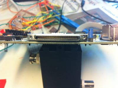
When building a board-to-board interface using the VHDCI connector, your options for male connectors are:
- Use Samtech part VHDCP-68-01-M-EM. Note! Apparently now discontinued. Requires a 0.8mm PCB. Body of the connector doesn't physically attach to the PCB, so you have to be very careful about disconnecting it in order to not stress your PCB traces. When used with the Atlys, differential pairs end up being split between the top and bottom layers, which feels a bit dirty but seems okay when I've tried it at 200 MHz.
- Use All Best electronics part R-HI-008068-2, which is presumably what Digilent use on their mating boards. Digilent now sell this connector for $9.49 (and seem to have discontinued the female connector). It is not stocked by any of the major distributors, but can be bought from the manufacturer; however it is very expensive in low quantities due to a $100 handling charge and an unspecified shipping charge.
The final option is to use a female VHDCI connector (which are much more common than the male) and a VHDCI cable. Digilent sell these, and they're fairly common on eBay. I don't really like the idea of long, thick cables connecting to my tiny, fragile interface board though!
HDMI
The reference manual states a few untruths about the HDMI interface. The Digilent test application uses an EDK-ed version of the XAPP495 code, and not the xps_tft core. XAPP495 does not provide an implementation of HDMI's EDID, so the dvi_demo may not work if you connect it to a source (such as some PC graphics cards) that require EDID. There are a couple of different solutions: setting the jumpers to allow for SCL/SDA pass-through (but this has some other caveats), using a DVI splitter cable to attach an extra monitor to the HDMI source, or implementing an EDID ROM. Please see my Improved XAPP495 design below.
Note that HDMI input J1 is disabled by default unless you install JP5, which is connected to the TMDS141 chip's output enable. This is not documented anywhere!
If you're new to ISE, here are the steps you'll need to take to try out XAPP495, or see below where you can download an
- Create a new project in ISE. Set the device to XC6SLX45-CSG324, speed grade -3.
- Add all of the Verilog (.v) files in the XAPP495 distribution to the project.
- Set either vtc_demo.v (colour bar generator) or dvi_demo.v (2x2 switch matrix) as the top module by right-clicking and selecting "Set as Top Module"
- ISE won't like it if you add both of the UCF files, so either add dvi_demo.ucf or vtc_demo.ucf to the project, depending on the demo you want to try. You might want to create two projects - one for dvi_demo and one for vtc_demo.
- Select the top module and Generate Programming File.
The vtc_demo should cause you no woe, but dvi_demo will probably require some reconfiguration of jumpers on the Atlys for it to work:
- Add jumper JP5 to enable HDMI input on J1
- Install jumpers JP6/JP7 to enable SDA/SCL pass through from J3.
- Install jumpers on the anonymous header labelled SDA/SCL next to J1 (they're called JP2 on the schematic, though). On the boards I've seen and heard about, these were supplied from the factory with jumpers connected, but installed incorrectly, shorting SDA and SCL together on both sides rather than passing them through. Check the schematic diagram to see if this applies to you and then rotate them if necessary.
There's a more thorough analysis of the Atlys HDMI situation on the timvideos wiki.
An explanation of the DDC control signals, which are used for EDID. Looking at the schematics, the PMODA HDMI connector (an output - the unlabelled one on the bottom of the board) has its SDA/SCL connected to JA-SCL/JA-SDA and, if you fit JP2, which is labelled as "SDA" and "SCL" on the PCB, PMOD-SCL/PMOD-SDA.
JA-SCL/JA-SDA go to C13 and A13 (on the FPGA). PMOD-SCL/PMOD-SDA go through the HDMI buffer and to HDMI input J1. This means that the DDC for input 1 is either left floating (if JP2 isn't fitted) or is connected to some FPGA pins and output PMODA.
HDMI OUT J2 has its DDC connected to TMDS-TX-SCL/TMDS-TX-SCL (D9 and C9). If you fit JP6 and JP7, these are connected directly to HDMI IN J3's DDC
As a result, switching options are limited! HDMI sources (inputs) must be connected directly to one of the outputs, or not at all, and the connections are fixed. However it would be possible to work around this by connecting the four appropriate pins on JP2, JP6 and JP7 to spare inputs (e.g. on the PMOD connector JB).
Note that if you are using HDMI DDC pass-through, you will need to set the corresponding FPGA pins (C13 and A13, D9 and C9) to high impedance in your constraints file or else they will load the bus.
XAPP495 ISE 14 compatibility
The XAPP495 examples were written for ISE12.x and are not compatibile with later versions - you will get the error "BUFIO2 has an invalid setting of DIVIDE by 2. This setting is not supported."
Xilinx forum user yetanotherid has provided a solution. Rather than using BUFIO2 to divide the 100 MHz system clock by 2, we now use a DCM (Digital Clock Manager) to generate the 50 MHz signal.
  // In vtc_demo.v, replace this code:

  BUFIO2 #(.DIVIDE_BYPASS("FALSE"), .DIVIDE(2))
  sysclk_div (.DIVCLK(clk50m), .IOCLK(), .SERDESSTROBE(), .I(sysclk));

  // With this code:

  wire clkfb;

   DCM_SP #(
      .CLKDV_DIVIDE(2.0),
      .CLKFX_DIVIDE(1),
      .CLKFX_MULTIPLY(4),
      .CLKIN_DIVIDE_BY_2("TRUE"),
      .CLKIN_PERIOD(10.0),
      .CLKOUT_PHASE_SHIFT("NONE"),
      .CLK_FEEDBACK("1X"),
      .DESKEW_ADJUST("SYSTEM_SYNCHRONOUS"),
      .DFS_FREQUENCY_MODE("LOW"),
      .DLL_FREQUENCY_MODE("LOW"),
      .DSS_MODE("NONE"),
      .DUTY_CYCLE_CORRECTION("TRUE"),
      .FACTORY_JF(16'hc080),
      .PHASE_SHIFT(0),
      .STARTUP_WAIT("FALSE")
   )
   DCM_SP_inst (
      .CLK0(clk50m),
      .CLK180(),
      .CLK270(),
      .CLK2X(),
      .CLK2X180(),
      .CLK90(),
      .CLKDV(),
      .CLKFX(),
      .CLKFX180(),
      .LOCKED(),
      .PSDONE(),
      .STATUS(),
      .CLKFB(clkfb),
      .CLKIN(sysclk),
      .DSSEN(1'b0),
      .PSCLK(1'b0),
      .PSEN(1'b0),
      .PSINCDEC(1'b0),
      .RST(1'b0)
   );

   BUFIO2FB #( .DIVIDE_BYPASS("TRUE") )
   BUFIO2FB_inst ( .O(clkfb), .I(clk50m) );
Improved XAPP495
The XAPP495 design does the bare minimum to demonstrate the HDMI receiver / transmitter concept. It fails to work for most people due to EDID issues, and is not completely compatible with modern versions of Xilinx ISE. I have fixed a couple of problems in the design:
- Fixed mixing of blocking/non-blocking assignments
- Fixed the BUFIO2 divide error
- Implemented EDID ROM for both HDMI inputs using the Hamsterworks EDID_ROM implementation, but with lower resolution EDID definitions taken from TimVideos' HDMI2USB.
You can download it from here:
- XAPP495 Fixed (20150515)
Some jumper setting is required:
- JP2 (labelled SCA/SCL) - these two jumpers must be set horizontally (your board may have been supplied with them set vertically)
- JP4 - install
- JP5 - install
- JP6/JP7 - remove
- JP8 - install
I've had reports that this worked, but I'm not able to confirm it myself as I no longer have my Atlys!
USB ports
Host
The manual and a close look at the board indicates that the USB host is controlled by a PIC24FJ192, while the schematic says it's a PIC32MX440F256H-40I/MR!
The PIC will load a bit file placed on a USB drive formatted with a FAT file system if jumper JP11 is closed. Note that it takes about 26 seconds for the load process to complete! LED7 will be stuck on while JP11 is closed, but the jumper can be removed once the FPGA has been initialised.
Some fine investigative work by Stromeko has revealed that only USB devices advertising a current consumption of 100 mA (or less) will work. If your device isn't working, check the USB descriptor on a computer.
The PS/2 interface provided by the PIC uses open drain ports, so it's necessary to provide pull-up constraints. Note that the manual is wrong - the PS/2 mouse clock and data pins are swapped. The following constraints are correct:
Net "PS2DATA" LOC = N18 | IOSTANDARD = LVCMOS33 | PULLUP;
Net "PS2CLOCK" LOC = P18 | IOSTANDARD = LVCMOS33 | PULLUP;
Device
The Atlys has a USB-serial device, which works fine, but for higher speeds consider using MakeStuff FPGALink. It is a library and firmware for the Cypress FX2LP USB controller (the "PROG" interface) that replaces Digilent Adept and provides an open source, cross platform bitstream upload facility and a high speed (40 MB/s) data transfer facility.
PicoBlaze
There's now a version of the PicoBlaze soft processor for the Spartan-6, but it didn't originally include the UART peripheral that came with the Spartan-3 core. I've fixed the UART so that it synthesises and runs on the Atlys and have written a small demo/framework design based on the old alarm clock demo. It's intended as a nice starting point for new designs that require PicoBlaze.
- Spartan 6 PicoBlaze demo (20110513)
Note that a new version of KCPSM6 has since been released, complete with UART, so you should drop the new files into this demo until I get around to updating it.
AC'97 codec
Predictably, the manual again has some grievous errors. The references to the 1/8" audio ports (J15-J18) are wrong (should be J4-J8), as is the codec (IC19 should be IC3). The FPGA pin assignments given in the diagram on page 14 are correct (N16, L13, T18, U17, T17), but those in the table on page 15 are wrong. This was probably copied and pasted from another board's manual and not corrected.
Digilent's built-in self test application has plenty of code for decoding and encoding AC'97 frames (ac97_if), and comprehensive example MicroBlaze C code for initialising and playing with the codec (ac97_if_00.c).
Digilent have now released a MicroBlaze design demonstrating just AC'97.
Jose Juan Garcia-Hernandez from Cinvestav Tamaulipas has written a VHDL implementation of AC'97 for the Atlys. It includes a demo that passes audio from line in to line out, and allows volume and channel to be controlled. He has kindly released it without restriction but asks for a citation if you use it.
Speed grade
It's impossible to tell because the Spartan-6 chip on the Atlys has a heatsink attached, but according to mrflibble, Digilent report that it's a -2. The BSB files that Digilent supply claims that it's a -3.
Other links
Stromeko has some interesting notes about the Atlys, including errata.
BASTLI has created an expansion board and turned the Atlys into a logic analyser called BitHound based on SUMP.
