20100803
Encode clock synthesis
My ADC board is partially built and ready to go, but I need to get something talking to it first! So, I've dusted off ISE Webpack and have started trying to get my development board doing things.
The first order of business: the ADC runs at a maximum of 65 MSPS, so I need to generate a sample clock for it. My development board has a 16 MHz oscillator, so I'll just multiply that by four to get 64 MHz, then see what happens when I connect that to an output pin.
I used the Architecture Wizard to generate a clock multiplier that did 4x multiplication. After that, instantiating it was as simple as:
	clock clock64 (
		.CLKIN_IN(clock_16),
		.RST_IN(RST_IN),
		.CLKFX_OUT(leds[3]),
		.CLKIN_IBUFG_OUT(CLKIN_IBUFG_OUT),
		.CLK0_OUT(CLK0_OUT),
		.LOCKED_OUT(leds[0])
	);
Now my leds[0] is on solidly, and leds[3] is blinking at 64 MHz!
Encode clock generation
The next step - the clock signal needs to use LVDS signalling.
Some Googling suggests that I should instantiate an output buffer using OBUF_LVDS, but this caused some errors. I poked through Language Templates and found an OBUFDS thing that looked like it might do the trick, and also save me from having to manually generate inverted signals:
	reg ltc_enc_data;

	 OBUFDS #(
      .IOSTANDARD("LVDS25") // Specify the output I/O standard
   ) OBUFDS_inst (
      .O(ltc_enc_p),     // Diff_p output (connect directly to top-level port)
      .OB(ltc_enc_n),   // Diff_n output (connect directly to top-level port)
      .I(ltc_enc_data)      // Buffer input
   );
Unfortunately, this caused an error, "Unable to combine the following symbols into a single DIFFSTB component:" Looks like it's because the outputs I've arbitrarily chosen are on bank 1 and the Spartan-3A only supports differential outputs on 0/2. Also, my board doesn't have a 2.5V supply! Let's try LVDS33 instead and hope that interfacing a 1.8V ADC to a 3.3V FPGA won't cause any smoke (note, will investigate this further before I connect them)
Well, that didn't make any difference. Maybe it is a bank thing, though it turns out that the pins I chose were both actually in bank 0. After some more head scratching, I found a pinout table in the Spartan 3A data sheet for my chip, which helpfully states that C11 and A11 are L07P_0 and L07N_0 respectively - I'll try moving the outputs to those. Success! Thanks for nothing, cryptic error messages!
So, the test - failure! I suspect this is because I'm not actually giving the buffer any data - I just stuck a '1' in there, but apparently LVDS doesn't like a complete lack of state changes at all! Maybe. So instead I used my 64 MHz clock to set a register based on the 16 MHz clock, and attached that register to the buffer:
	reg ltc_enc_data;

	 OBUFDS #(
      .IOSTANDARD("LVDS_33") // Specify the output I/O standard
   ) OBUFDS_inst (
      .O(ltc_enc_p),     // Diff_p output (connect directly to top-level port)
      .OB(ltc_enc_n),   // Diff_n output (connect directly to top-level port)
      .I(ltc_enc_data)      // Buffer input
   );

	always @(posedge CLKFX_OUT)  // 64 MHz clock
	begin
		ltc_enc_data <= CLK0_OUT; // 16 MHz output from DCM
	end
The result:
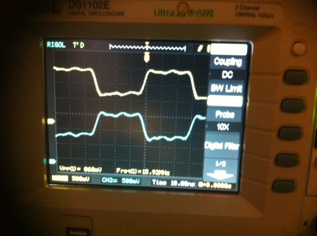
All this register twiddling seems pretty redundant - it also works if you set the buffer input to CLKFX_OUT, which results in a 64 MHz output.
Now, let's consider the voltages. At 64 MHz, my oscilloscope reports a Vpp of 1.14V, while at 16 MHz it was 860 mV. In fact at 16 MHz, Vmax = 1.74V, Vmin = 860 mV. Comparing this to my ADC's data sheet: ENC+, ENC- to GND must be between 0.2 and 3.6 V. Now that I think about it, the ADC's analogue supply is 1.8, while its digital supply is 3.3V! So this all seems to be spot on.
ADC configuration
I've wired the ADC up to support configuration via SPI, so my FPGA needs to blat configuration words at it every whenever. Specifically, I need to be able to set the output mode to 2-lanes, 14-bit serialisation (unless I decide that 1 lane is fine - I suspect that at full rate my Spartan-3A might conk out though). Also there's a digital output test mode, which sounds useful for verifying my LVDS deserialisation code, once I've written it.
fpga4fun.com has an SPI example, but it's not nicely packaged into a module. opencores.org has one called simple_spi that is based on my old friend, the MC68HC11! I plonked that into my project and managed to get the test bench to pass (though there seemed to be errors in one of the files, but they were easily fixed). I've no idea what it's doing or how it works at this stage.
LVDS deserialisation
To do: create something based on the Xilinx application note that deserialises a single lane LVDS signal into 12-bits, but expanded to 14-bits and taking inputs from two lanes simultaneously, which shouldn't be a giant leap. The only problem is that the code is a bit beyond me at the moment, and it's written in VHDL. I'll attempt to port it to Verilog, which should help me to understand how it all works.
Output data
At this stage, I'll aim to capture n samples into RAM and then dump them out of the serial port so that I can first verify the test patterns, and later capture samples for analysis on my computer. This means I have another to do: figure out how to interface with the evaluation board's serial port. I suspect that one of the Avnet application notes that deal with soft cores might help here (though I can't follow their tutorials because they require the Xilinx EDK, and I don't have a license).
